Digital Design & Verilog
Build strong fundamentals in combinational logic, sequential design, FSMs, and synthesizable RTL.
Explore path Banzs ASIC FlowBY BANZS TEAM
RTL → GDSII · Foundation to Advanced
A mentor-led, hands-on workshop covering Digital Design, Verilog, Verification, Synthesis, Static Timing, Physical Design and Signoff—with 160+ interview-style assignments.
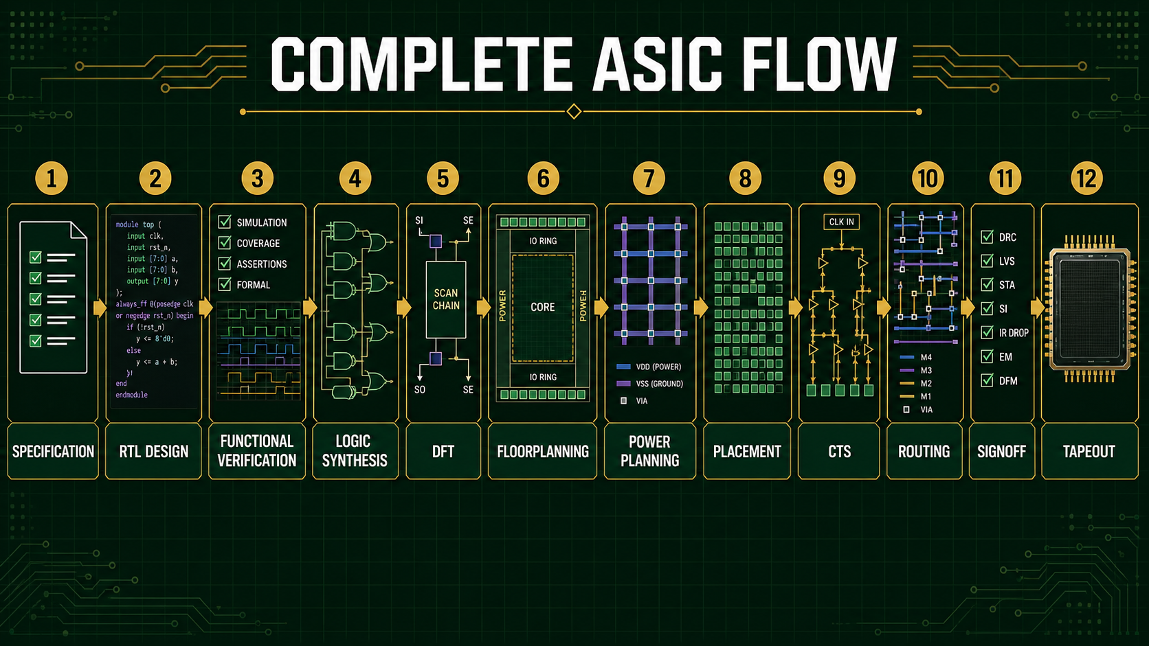
Complete workshop map
This 2D technical map connects front-end design, verification, implementation and signoff. Select any learning path below to study each stage in depth.
Structured learning paths
Every module connects to the real chip-design lifecycle, so you understand not just the tool—but why each step matters.
Build strong fundamentals in combinational logic, sequential design, FSMs, and synthesizable RTL.
Explore pathLearn testbench architecture, assertions, coverage, debugging, and practical verification thinking.
Explore pathTurn RTL into optimized gates while reasoning about constraints, timing, power, and area.
Explore pathMove from floorplan through placement, CTS, routing, optimization, and GDSII generation.
Explore pathMaster setup, hold, clock paths, constraints, OCV, and signoff-quality timing analysis.
Explore pathUnderstand DRC, LVS, antenna checks, and the final quality gates before tapeout.
Explore pathRecommended roadmap
Follow one connected path from a design idea to a manufacturing-ready layout. Each stage gives you the foundation for the next.
Get the learning roadmapFlagship workshop
A practical, mentor-led program built around the complete flow. Learn the concepts, read real reports, and connect every implementation stage.
Write clean, synthesizable hardware
DesignTest functionality, assertions and coverage
VerificationMap RTL into optimized technology gates
SynthesisPlan die, core, I/O, macros and power
FloorplanBuild a balanced, low-skew clock tree
ClockingRoute, verify signoff and deliver GDSII
TapeoutWhy Banzs Team
Clear explanations, practical context, and a connected curriculum for learners who want to understand how chips are actually built.
Learn how front-end decisions affect timing, power, area, and physical implementation.
Move beyond definitions with report reading, constraints, debugging, and implementation scenarios.
Ask better questions, build stronger fundamentals, and prepare for real VLSI work.
Your ASIC journey starts here
Join Banzs Team and learn the path from RTL to reliable silicon.
Start learning today